Caption
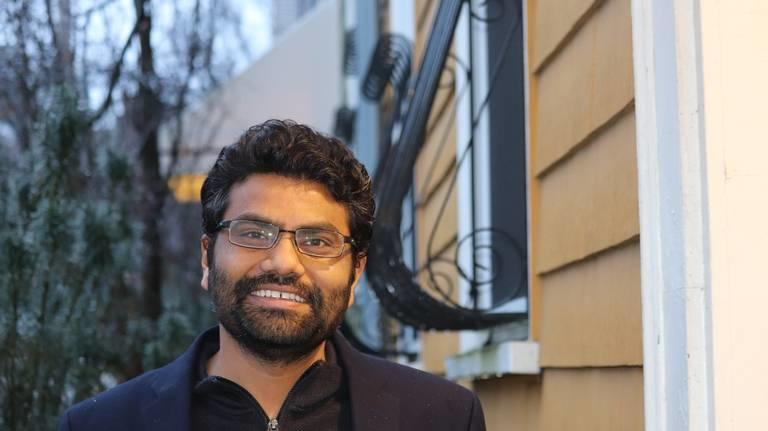
Prashant Patil is founder and CEO of Micromize, a semiconductor manufacturer that specializes in energy-efficient electronics for wearables and mobile devices.
As the country focuses on increasing the manufacturing and packaging of microchips domestically for national security, local support convinced a semiconductor manufacturing company to choose Columbus as its headquarters.
Micromize, a semiconductor manufacturer that specializes in energy-efficient electronics for wearables and mobile devices, recently announced it will bring its operation to Georgia with Columbus as its home base and utilizing Georgia Tech for its research and development.
The move comes as a result of the work done by the coalition called Chattahoochee Hub for Innovation and Production of Semiconductors — more commonly known as CHIPS4CHIPS (C4C). The group, led by the United Way of the Chattahoochee Valley, joined in a partnership with other local leaders and Georgia Tech to bring Micromize to Georgia.
This local support was instrumental in the company’s decision to come to Columbus, founder and CEO Prashant Patil told the Ledger-Enquirer, because it’s necessary to grow the industry in the region.
The Ledger-Enquirer spoke with Patil about the importance of the semiconductor manufacturing industry, what it means for national security and why Columbus was a good location to bring Micromize.
The answers have been edited for clarity and length.
A: The company was founded in 2020 to commercialize the technology I developed during my PhD at MIT.
We look at all the electronic devices: smartphones, smartwatches, computers. They are getting smaller and smaller. And to make them smaller, you have to reduce the size of the electronics inside it.
The devices we’re seeing now can no longer be miniaturized because of the limitation of the technology. Now, we have this new technology that can further reduce the size of the electronics that goes into this device.
So, imagine a smartphone. With smaller electronics in use, we now have more space for the battery. You can extend battery life.
The technology was developed at MIT, and we filed patents. When I graduated from MIT, I decided to work on commercializing this technology.
A: There are multiple reasons. The first one is national security.
If you think about any electronic device — router, smartphones, smartwatches, tablets, laptops — they all have this silicon chip inside it that carries a lot of data. We’re all worried about our privacy, and all these devices connect to the internet.
There is a program that can read the data on the chip and send it to a server. That’s a security issue because now you have devices that are basically taking all this data and putting it aside, which then can be used for adverse situations.
Now, in the US, we make these chips but a lot of the packaging happens outside the country. And many chips are also made outside the country.
Once you make these chips and send them outside for packaging, we don’t know what we are getting back because the chips are so small. It’s not like a metal box you can open and see what’s inside.
So, once it comes to the U.S., all these devices become a security vulnerability because we don’t know what is actually in the chip. We don’t want to rely on an outside vendor to make these chips for us.
That’s on the security side, but another reason is if you look at how things are moving on the consumer side.
Artificial Intelligence (AI) is booming, and we need AI hardware, which again are these chips. If we don’t make the chips in the country, then we are again relying on an outside country to make these chips for us, which are an integral part of human society.
They are in anything from cars to toothbrushes to anything that has some level of intelligence. We want to stay ahead to make sure that we make those chips in the US and not rely on outside manufacturing.
A: For prototyping and R&D work, we rely on something called a cleanroom, or micro fabrication facility. There are cleanrooms across the U.S. There’s one at MIT, and there’s one at Georgia Tech.
There were certain capabilities that we needed that were available only in the cleanroom at Georgia Tech. And that’s why we have moved to Georgia Tech to use their facility.
Through Georgia Tech, we got connected to ATDC (Advanced Technology Development Center), which is the state technology incubator program. We got a lot of mentorship, which led to me meeting with Dr. Ben Moser, who was heading C4C.
The support we got from the city and Columbus mayor showed us that a commitment to build a semiconductor ecosystem.
And given that it’s close to Atlanta and Georgia Tech, we can do our R&D work.
Columbus has proximity to Fort Moore, so recruiting-wise it’s easier because there’s already talent available. The cost of living is low, and we have support from this city.
A: If you look at the money that the government is putting in the economy. To get that kind of federal grant, the application becomes really strong when you’re working with a partnership instead of just applying on your own.
So, it helps both Micromize and C4C to file together for these grants.
Micromize is the first company currently located in Columbus, and C4C is working with other companies to attract them. Once you build an ecosystem where there is one company who’s building the chips, then Micromize can take that chip and package it.
We become the vendor for packaging, and they become our customer for packaging. You can now start to see how different companies working in different aspects of the industry can come together in one location to help each other.
That is the other important part for us deciding to come to Columbus because the city is working on building a semiconductor manufacturing ecosystem. And once we do that, we don’t have to go anywhere else to find our customers because we can find it in Columbus.
A: Our plan is to really start building the factory in Q1 of 2025.
The first factory will be the pilot factory that becomes a model factory for replicating or building larger. The first factory will employ about 15 to 20 people with a pay scale of around $125k per person.
A: Traditional semiconductor manufacturing packaging is a process that requires a lot of chemicals and consumes a lot of water. And it’s capital intensive.
The technology we have developed is environmentally friendly. It’s a chemical free process. And environmentally friendly. We’ve reduced water consumption by 90%.
And our capital investment to build the factory is about 1/10 of what the traditional cleanroom, like the one at Georgia Tech for example, cost. That is why, even though we’re a startup, we can start ramping up manufacturing much earlier than any other semiconductor manufacturing company.
This story comes to GPB through a reporting partnership with Ledger-Enquirer.